Proper decoupling practices, and why you should leave 100nF behind
Ever wondered why 100nF is a go-to value for decoupling capacitors? This number has pervaded in datasheets and electronics advice going back to the 1980s, and is still widely present in the datasheets of modern components. Folks are out there sprinkling 100nF capacitors on their boards like seasoning, and when they decide 100nF isn’t enough, they inevitably recommend the big/little practice, e.g. 1uF + 100nF in parallel.
Unfortunately, 100nF kinda sucks, and this common decoupling practice is incredibly outdated.
To understand why this practice is so outdated, we need to first consider the problem that decoupling solves and how it solves it. I want to be thorough here, so grab a beverage, put your feet up, and prepare for the long-haul.
One of the easiest contexts to explain this topic in is digital electronics, such as decoupling a microcontroller. A microcontroller can be crudely and simplistically described as a big ol’ heap of transistors. Every time one of those transistors needs to change state, a current flows into or out of the gate in order to charge or discharge its gate capacitance. Most of these transistors are arranged in CMOS circuits, and these circuits also tend to have a small amount of shoot-through current during the rising and falling edges of switching, while the transistors are neither fully on nor off. The amount of current associated with a single switching event is small, but there are a lot of CMOS gates in a microcontroller, and they’re constantly switching on and off, so it adds up once you start measuring it at the power pins.
This type of dynamic load current is numerically measured as dI/dt (pronounced “dee-eye dee-tee”), which comes from Leibniz’s notation in calculus. If you didn’t study calculus, or had a bad teacher for calculus like I did, don’t worry. Put plainly: it is the rate of change of current with respect to time, i.e. the change in current (delta I) divided by the change in time (delta t). For example, if a device goes from drawing 1A to 3A in the space of one second, that’s 2A/s of dI/dt. If a device goes from drawing 50mA to 45mA in the space of one nanosecond, that’s -5mA/ns of dI/dt (often just referred to as 5mA/ns, without the minus sign, since it’s the magnitude of change we’re typically interested in).
A common misunderstanding about dynamic power delivery in digital circuits is that the frequencies we will be dealing with are dictated by the clock frequency. This is actually not true at all. What matters is the rise and fall time.
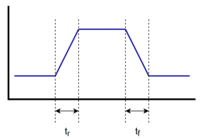
Typically we measure these times using the 10-90 rule, i.e. how long it takes to go from 10% signal level to 90% signal level, or vice versa. We can convert a given rise or fall time to a bandwidth, i.e. the maximum frequency component needed to produce a given rising or falling edge at that rate. If you’re familiar with Nyquist frequencies, it’s the same idea. You’re looking at the signal in the frequency domain and figuring out what the highest frequency component of the signal is. A general rule of thumb is that the bandwidth in GHz is equal to 0.35 divided by the rise time in nanoseconds, so a 1ns rise time has an associated bandwidth of around 350MHz. This relationship between rise time and bandwidth is critical, because it tells us what frequencies we’ll need to deal with in our decoupling.
The clock frequency only tells us how frequently an edge occurs. The rise/fall times tell us what frequency components will be present during edges. For an extreme example, if you have a 1Hz clock signal with a 350ps rise time, your circuit must be carrying frequencies up to 1GHz in order to achieve that rise time.
In an ideal world the current that your device demands would be sourced from the power supply. The problem is that your power supply is all the way over there, and the journey is perilously mired in parasitics. The traces between your device and the power supply aren’t perfect conductors - every single conductor in your circuit has some amount of parasitic resistance, inductance, and capacitance. At DC the resistance dominates and the parasitic inductance and capacitance don’t matter, but the dynamic currents (dI/dt) of a load are, by definition, an alternating current.
Parasitic inductance is typically the biggest factor here. Inductance causes a voltage drop proportional to the dI/dt; formally, we say V = L ∙ dI/dt, i.e. the voltage drop (in volts) is equal to the inductance (in henries) multiplied by the rate of change of current (in amps per second). This is why a dynamic current load manifests as voltage noise on the power rails. The amount of parasitic inductance in a trace is related to its geometry - the width and thickness of the copper, the length of the trace, and the height of the trace above the return path (ground plane below) all contribute. For example, a 1mm wide, 5cm long trace on a typical 4-layer PCB might have around 50nH of inductance. If your device has a dI/dt of 2mA/ns, that parasitic inductance will cause 100mV of voltage noise across the trace. You can find calculators online to estimate trace inductance if you want rough numbers. For more precise numbers you need a field solver, which is far out of the scope of this post.
The voltage on the trace is also affected by simple resistive behaviours (V=I∙R, so a change in I produces a proportional change in V), and capacitive behaviours (I = C ∙ dV/dt). I won’t go into all the mathematical and analytical details here (although I will explain in more detail later), but it is possible to combine all of these measurements into a single measurement called impedance, measured in ohms. Put very simply: impedance sums the “resistance-like” effects of resistance, inductance, and capacitance at a given frequency together into a single measurement. We usually plot impedance vs. frequency, since it is frequency-dependent. The impedance tells us the relationship between voltage and current we should expect at a given frequency, and it follows the familiar Ohm’s law relationship of V=I∙|Z|, where |Z| is impedance (instead of resistance in the traditional formula) in ohms. For example, if a circuit path has an impedance of 50Ω at 10MHz, an AC current of 2mA at 10MHz flowing through that path will produce a 100mV voltage difference across it.
Side note: as much as it would be convenient to say so, it is not correct to describe impedance as “frequency dependent resistance”, since resistance is already frequency-dependent due to the skin effect, and while impedance does behave like a resistance in some regards it does not in others.
At low frequencies and DC, the impedance of a PCB trace is typically very low and dominated by the resistance of the path. As the frequency climbs, the dI/dt increases, leading the inductance to be a greater and greater factor, increasing the impedance. The resistance itself also climbs due to the skin effect, contributing to the total impedance. As such, the impedance of a power delivery path typically starts out low at low frequencies and climbs as the frequency increases.
A high impedance power delivery path causes a range of problems. First and foremost, it reduces power delivery network (PDN) integrity. When a device has a sudden demand for current, a PDN with high impedance will suffer a voltage drop across it, leading to an unstable supply to the load. In the context of digital devices, this may lead to glitching. In the context of analog devices, this leads to noise. This voltage noise generated by one device’s dynamic current demands may affect other devices on the same power rail, too. In addition to the direct problem of PDN integrity, having your large dI/dt flow across the board can lead to signal integrity and electromagnetic interference (EMI) issues. A change in current through a trace manifests as a change in the electromagnetic field around that trace. When a changing electromagnetic field cuts through other traces, electromagnetic induction occurs. We refer to this as crosstalk. A high dI/dt through a trace causes large perturbations in the fields around it, increasing the likelihood and magnitude of crosstalk. In addition, the fields may spread out and cause electromagnetic interference (EMI). We want to avoid these problems.
The comparatively high impedance of the power delivery network at high frequencies is the problem that decoupling aims to solve. We want to ensure that fast dynamic current demands do not impact the stability of the voltage rails, and we want to contain the high frequency currents so they don’t spread out and cause crosstalk and EMI. We can do this by using a capacitor as a low impedance path for high frequency currents. Rather than having both the high- and low-frequency currents flowing through our entire power delivery network, we decouple the high-frequency currents so that only the lower frequency currents need to flow all the way back up to the supply.
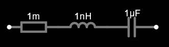
We can model the behaviour of a decoupling capacitor in a power delivery network using an impedance network. This behaves almost identically to a resistor network. If you have several current paths to a load, each with its own impedance, you can use Kirchhoff’s circuit laws to model how much current flows through each path. Here’s an example of a 9 ohm impedance and 1 ohm impedance in parallel, with a 1:9 ratio of current sharing:
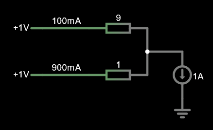
Note that resistors are being used as a proxy for impedance here, just to demonstrate that the current sharing works the same way.
To understand how the capacitor acts as a low impedance source for high frequency currents, we need to understand how its impedance changes with frequency. The impedance of an ideal capacitor (i.e. a capacitor with no parasitic resistance or inductance) is given by the following formula:
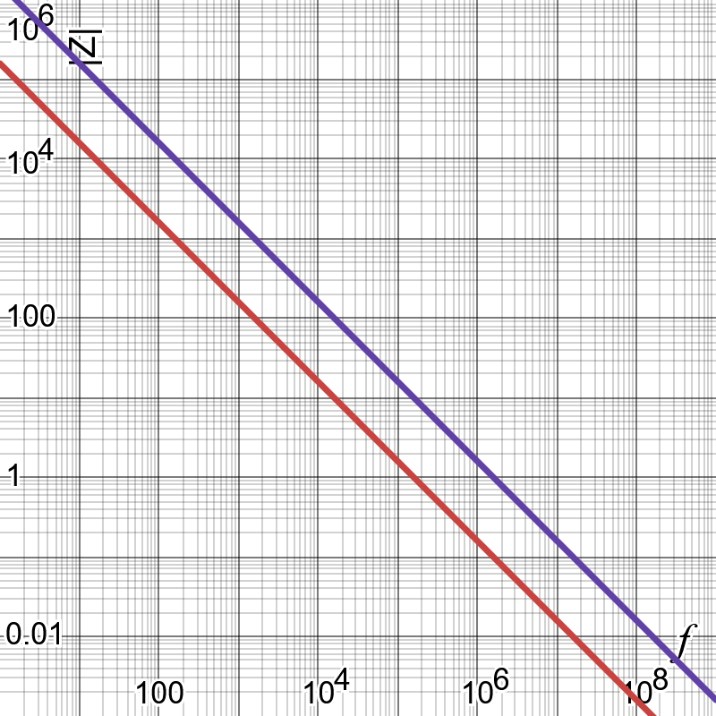
Where f is the frequency in Hz and C is the capacitance in Farads. From this, we can see that a perfect capacitor has infinite impedance at DC (f=0), which means no current flows through it at DC. The impedance of the capacitor then falls toward zero as the frequency gets higher and higher. The rate at which it falls towards zero is proportional to the capacitance.
Note: This is a simplified formula. The complete formula involves complex numbers that describe a phase relationship between inductance and capacitance, but for the purposes of this article we can skip that complexity (pun intended) and stick with the simple version. However, it is worth noting that the phase relationship between inductance and capacitance does become important when the magnitudes of inductance and capacitance are similar, as we will see shortly.
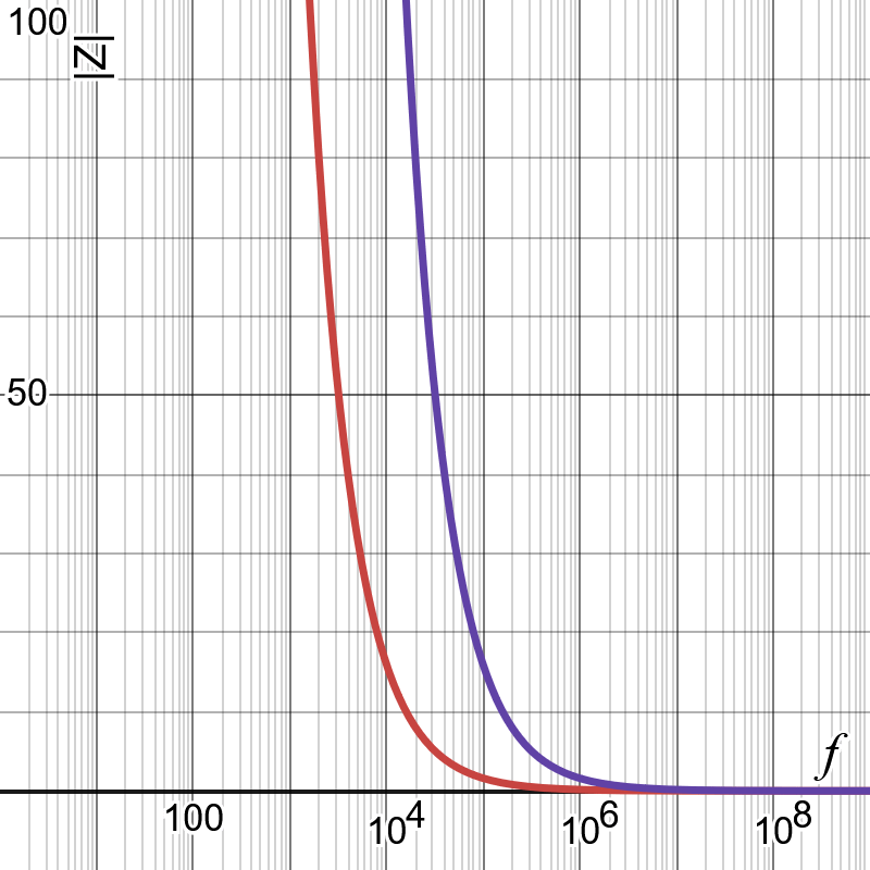
We usually show this on a log-log plot of impedance (|Z|) versus frequency (f), such as the following plot for an ideal 1uF capacitor (red) and an ideal 100nF capacitor (purple):
For the purposes of clear understanding, it may be beneficial to also see the graph with a linear vertical axis:
We can see from this that a decoupling capacitor provides a low impedance path at high frequencies, and a high impedance path at low frequencies. This is the opposite to a typical power delivery trace, where the impedance is low (approaching the series resistance) at low frequencies, and high at high frequencies. Combining the two gives us the best of both worlds.
Furthermore, the larger our capacitance, the lower the impedance at a given frequency, at least for an ideal capacitor. If we think about this in the context of an impedance network, as depicted above, we know that we would like to have as much high-frequency current as possible flow through the decoupling capacitor as possible, which we can achieve by making the capacitor as low impedance as possible. This leads us toward the conclusion that a larger value capacitor is better for decoupling than a smaller value, due it providing a lower impedance.
Unfortunately, real components are not “ideal”, and in the real world we have parasitics to contend with. Capacitors have some equivalent series resistance (ESR) and some equivalent series inductance (ESL). For example, we might model a 1uF capacitor with 1mΩ of ESR and 1nH of ESL as follows:
The impedance of an ideal inductor is given by the following formula:
Where L is the inductance in Henries. It should be clear from this formula that the impedance of an inductor rises linearly with frequency, with a gradient proportional to the inductance.
Note: Again, this is a simplified version of the formula, with the complex portion skipped. It is sufficient to illustrate the points in this post.
If we sum the three series impedances together, we get:
If we graph this for our example 1uF capacitor, with 1nH of parasitic inductance and 1mΩ of parasitic resistance, we get the following:
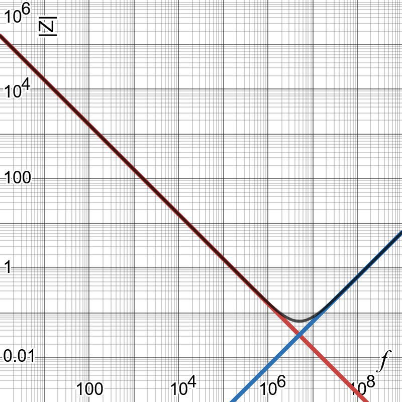
The red line shows the impedance of the capacitance. The blue line shows the impedance of the parasitic inductance. The two cross over at around 5MHz; we call this the self-resonant frequency (SRF) of the capacitor. The black line shows the overall impedance of the capacitor, i.e. the sum of the two impedances. This parasitic inductance prevents real capacitors from being as effective at very high frequencies.
Now let’s look at what happens if we reduce the parasitic inductance by a factor of ten:
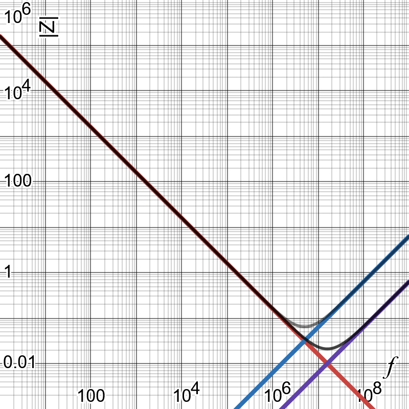
The lower inductance (purple line) shifts the self-resonant frequency higher and allows for a lower impedance at higher frequencies. This fact is absolutely critical to good decoupling. The more inductance you have in your decoupling path, the higher its impedance will be at higher frequencies. This is why you must place your decoupling capacitors as close to the load as possible, ideally across adjacent ground and power pins in the case of an IC. The shorter the loop, the less parasitic inductance in the path, and the better your decoupling will perform. This is not the only factor though, as we will see shortly.
It is worth noting that the series RLC model is simplistic. In practice, the parasitic resistance varies quite a bit with frequency, and the effective inductance and capacitance vary a little with frequency too. There is also some resonant interplay between the capacitance and inductance, which is better described by the complex form of the equations that I skipped over. The details of this are beyond the scope of this blog post. For now, the important part is that we have this V-shaped plot, where the impedance of the capacitor drops as we approach the self-resonant frequency, then climbs again as the impedance of the parasitic inductance becomes the dominant effect.
We can see this same effect in a real capacitor, albeit with a slightly different shape due to the aforementioned frequency-dependent phenomena:
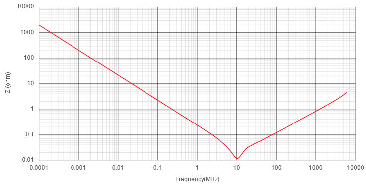
This graph was produced using the Samsung WebLib MLCC tool, and shows the impedance profile of a CL05A105KA5NQN 1uF 25V 0402 capacitor.
You may notice that there’s a “dip” around the self-resonant frequency which doesn’t appear in the model graphs. This is where that phase relationship between inductance and capacitance becomes apparent, and where the simplified equation I showed doesn’t quite match the more in-depth model. Luckily we don’t have to worry too much about it for the purposes of this blog post, because manufacturer-provided impedance plots show us the real behaviour, incorporating properties that go beyond even the complex impedance model.
Now let’s add a plot for another capacitor that has the exact same specs but in 0603 - the CL10A105KA8NNN.
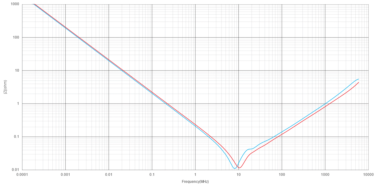
The blue line here is the 0603 package, the red is the 0402. Notice how the 0603 package capacitor’s SRF is shifted left, and its impedance in the inductive region (right hand side) is higher. This is due to higher parasitic inductance - the 0402 has around 320pH of parasitic inductance, whereas the 0603 has around 475pH of parasitic inductance. The parasitic inductance in a ceramic capacitor is almost always proportional to its physical size. I have previously published rules of thumb for parasitic inductance versus package size, and the correlation is strong.
The importance of the capacitor package size does double duty here. Not only does the capacitor itself end up having lower parasitic inductance, but the smaller size often allows you to reduce the length of the traces between it and the load, thus reducing the overall loop size for high frequency currents. This minimises the impedance of the decoupling path, improving PDN integrity and confining fields that would otherwise spread out and cause crosstalk or EMI issues.
One thing you might notice from the graph above is that the 0603 package capacitor has slightly lower impedance on the left side of the graph, at frequencies below its SRF. This is due to DC bias derating - a topic I covered in detail as part of my Notes on capacitors, part 1: ceramics & MLCCs post. In short, class 2 ceramic capacitors (X5R, X7R, etc. rather than C0G/NP0) suffer from DC bias derating, whereby the effective capacitance drops as the DC voltage across the capacitor increases. This phenomenon is directly tied to the volume of the dielectric material within the capacitor, so physically larger capacitors are generally able to provide more capacitance at a given higher DC bias voltage. The graphs above were generated for a DC bias of 3.3V, which results in effective capacitances of 785nF and 680nF for the 0603 and 0402 package components respectively. If you think back to the equation for capacitor impedance from earlier, this explains why the 0603 part has a slightly steeper downward gradient.
Note: bias derating only applies to class 2 ceramic capacitors, not other types of capacitors. But these are the type we tend to use for decoupling in most cases.
At this point, you might be wondering what we’re supposed to do about frequencies in the hundreds of MHz or even GHz. You may also be wondering why I largely glossed over the third of the parasitic properties within your board traces: capacitance. Well, here’s where those two details combine. Your power delivery traces couple capacitatively to the ground plane beneath them (you are using ground planes, right? if not, please go watch The Extreme Importance Of PC Board Stackup by Rick Hartley… or just go watch it anyway, because it’s the best electronics talk I’ve ever seen, and everyone needs to see it) and this interplanar capacitance acts as inbuilt decoupling within the board. The amount of capacitance is very small, but it is distributed across the board and fairly effective at decoupling very high frequency currents as long as your board stackup is good. The exact details here get very involved, requiring the use of field solvers to model properly, so I won’t get into that particular rabbit hole here.
Still with me? Good, because we’re finally in a position to talk about why 100nF is so outdated. Here’s an impedance plot for the two capacitors we already discussed, plus a 100nF 0402 capacitor (red trace).
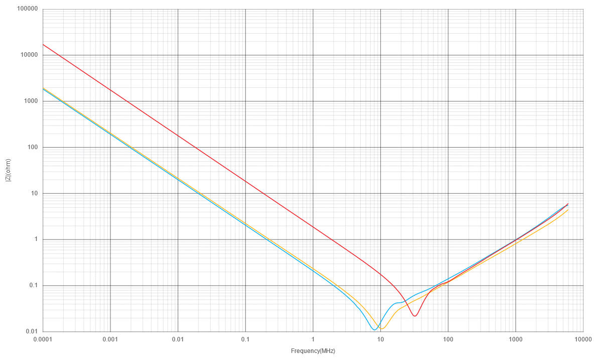
Well, uh, it’s ok at about 25-40MHz, I guess? Assuming, that is, that you’re using 0402 and not a larger package with more inductance. And that the parasitic inductance of the traces between your IC and the capacitor is negligible (hint: it isn’t).
Obviously this just plain sucks compared to the 1uF capacitors, so why on earth has 100nF been the recommended decoupling capacitor for the last 40-something years? Why was it ever considered good?
The answer boils down to a few different technical, financial, and human reasons.
Back in the 80s, ceramic capacitors weren’t anywhere near as good. They had much lower capacitance density, worse DC bias characteristics, their impedance was much higher, and good ones cost more money. Modern MLCCs are orders of magnitude higher density, they’re heavily mass-produced, and the unit cost has gotten so low that there’s no point comparing the pricing between parts for common values at low voltages. 100nF became popular at the time because it was a common, easy-to-remember value part that had good enough DC bias properties and impedance for decoupling the emerging low-cost CMOS devices of the time, and it didn’t cost a lot.
This is also where the infamous big/little practice arose. When 100nF wasn’t enough, you’d add a 1uF capacitor in parallel. The reason for doing this back then was because you couldn’t get 1uF of low impedance capacitance. You couldn’t fit 1uF in a small package, so the parasitic inductance was high and it didn’t make for a very good decoupling cap. Now? It’s trivial. In a recent design I needed a decoupling capacitor for a 3.3V microcontroller, so I picked the CL05A106MQ5NUN. This 0402 capacitor has around 3.5uF of effective capacitance at 3.3V bias. It costs $0.0041/pc (yes, that’s zero point four one pennies) from LCSC at the time of writing, and you can buy a full reel of ten thousand for about $20. This isn’t necessarily the most optimal part here, but it’s way better than a 100nF. For most low voltage power rails there’s no benefit at all from placing a small (<1uF) decoupling capacitor and then a large (>1uF) decoupling capacitor next to that. Since the cost of the parts is so incredibly low, it’s often more expensive to place two parts than to just place one higher density part, either due to the cost of the parts themselves or the additional assembly fees and board size increase. The parasitic inductance in the traces going to the further away capacitor ends up being much greater than the parasitic inductance in the capacitors themselves, so the effective SRF of the further away capacitor shifts lower, making it less effective for decoupling. To make matters worse, modern MLCCs are so incredibly low impedance that placing two very close together can lead to undamped resonances, leading to an increase in noise at certain frequencies. The details of this are beyond the scope of this blog post, but it’s a topic that you should be able to find information on with a quick search (even with the miserable state of search engines these days) if you’re interested.
Another difference between now and then is the rise and fall times. Modern commodity ICs have very fast rise and fall times compared to equivalent commodity ICs from the 80s. This is partly due to more modern MOSFET construction techniques that improve switching speeds and efficiency, but also came as a side-effect of die shrinks, where manufacturers use physically smaller transistors in order to squeeze more chips out of a silicon wafer. As a result, the dI/dt generated by your average digital IC has skyrocketed in the past 40 years. The parasitic inductance in your PCB traces, on the other hand, remains immutably governed by electromagnetic field physics, and hasn’t changed much. If you take a circuit design from the 80s or 90s, made with parts from that era, and measure its EMI, it probably won’t look all that bad. If you take the exact same circuit design and replace the ICs with modern equivalents that have undergone die shrinks, suddenly the EMI will look a lot worse. The bandwidth your average electronic device has gone up a lot over time, simply due to die shrinks. There are simply more high frequency currents flying around your board today.
“But Graham,” I hear you protest, “I see these practices recommended in vendor’s datasheets all the time! Surely they can’t be wrong? They’re professionals!”
This is, to a certain extent, an example of the (probably apocryphal) parable of the five monkeys, in which a practice or rule of thumb becomes important and reliable for good reasons, but pervades long after the practice becomes outdated because nobody remembers why it started in the first place. But to write it off as only that would be overly cynical.
I personally prefer to be a bit more charitable. I think this practice has pervaded because we all have a certain amount of cognitive bandwidth that we can allocate to each task, and one of the key strategies we have as humans for completing those tasks is to eliminate unnecessary cognitive load where we can. The 100nF value for decoupling became so entrenched because it works well enough* most of the time, so you don’t need to even think about it. By eliminating trivialities you can focus your brain-juices, spoons, or whatever else you want to call them on more challenging tasks.
As a corollary to this, most people don’t spend years digging into the minute details of capacitor properties, materials, and related physics phenomena. I did because my ADHD-riddled brain gets fixated on weird things, but not everyone wants or needs to know the gritty details behind every little thing, and that’s fine. In fact, that’s good and literally mandatory for us to function. If everyone was compelled to understand every detail of every device and system around them we’d all be crushed under the mental weight of it all. This applies to everyone, including the folks who write IC datasheets, and I want you to feel confident in ignoring their outdated advice not because they’re stupid, but because they just haven’t gotten around to updating their understanding and are sticking with a practice that feels safe.
Now, when I said that 100nF “works well enough” above, what I really mean is your circuit usually doesn’t completely break if you use a 100nF decoupling capacitor. But given that the cost to use a larger, better capacitor is effectively nil in most cases, you can keep experiencing that exact same level of cognitive load avoidance by just using 1uF or 2.2uF instead, in the smallest capacitor package that is practical for the voltage and assembly constraints you have, and placing it right up against the power pins. It’s free real estate, or something.
There are two cases where I would recommend caution:
- If you have a lot of devices powered off a single rail, placing lots of high-value decoupling capacitors will add up, so pay attention to inrush current. If you’re sticking 10uF decoupling caps on 20 devices then that’s 200uF. Maybe dial it back a smidge.
- Don’t put a bunch of high-value MLCCs really close to the output of a linear regulator or a switching regulator’s feedback network. This reduces the phase margin of the control loop. Consult the datasheet and the part vendor’s simulation tools for exact details, but as a rule of thumb physically moving the large MLCCs away from those areas by a small distance will drastically improve the phase margin, because the parasitic inductance in the traces acts to decouple that extra capacitance from the control loop.
I had planned to finish this piece off by going through some examples of cases where you might want to buck the trend and use multiple capacitors or smaller specialised capacitors, such as combining dielectric classes, but honestly if you’re in that camp then you probably already know what you’re doing anyway, and this post is far too long as it stands. It has taken me literal years to write a coherent version that didn’t get lost in the weeds. In fact I’m so happy about completing this post that I actually went and made myself a nice dinner to celebrate.
I shall see you all in the year 2055 when I have to write a companion piece called “… and why you should also leave 10uF behind”.
Thanks for reading this post! If you enjoyed it and want to say thanks, consider purchasing some of my amusing warning stickers. They’re 100% guaranteed to not to cause superpowers in sea creatures.