A neat trick in OCP Grand Teton’s power distribution design
Back in August I did a stream on Twitch where I dug through the OCP Grand Teton server chassis design. The Open Compute Project (OCP) is an organisation that works to design and publish open server standards. Their projects cover all sorts of datacenter tech, including entire server platforms. Many of their projects are published with collateral, i.e. the design files for the platform, including entire sets of schematics, PCB designs, documentation, mechanical drawings, etc.
OCP Grand Teton is a dual-blade chassis design that supports both AMD EPYC and Intel Xeon blades, with a PCIe 5.0 crossbar switch that allows the nodes to communicate with eight OCP NIC 3.0 slots, eight E1.S NVMe storage slots, and eight PCIe 5.0 expansion cards. It was designed by Quanta, for Meta (Facebook), and released under OCP license. If you want to download the collateral files, go to the OCP website, go to the Contributions Database, and search “grand teton”. One of the results will have a grey button that says “View available design collateral”. Click that button (not the result title) and then click the download link it reveals. The design files can be viewed with the OrCAD X Free Viewer, which includes Capture Viewer and PCB Editor Viewer, although most of the designs include a PDF of the schematic and gerber files if you’d prefer not to use Cadence’s software.
One of the boards I was looking at in the stream was the power distribution board. This board takes in 51-54V and produces 12V for the blades. It is capable of delivering either 3500W or 3900W of average continuous power depending on the configuration. The peak design current on the low side (12V) is 344A, which translates to about 80A on the high side. That’s a lot of current, and they manage to fit this into a board that’s just 150x330mm in size. Part of that comes down to it being a 10 layer board, but there’s some trickery afoot too.
The actual power conversion is achieved by three 1300W DC-DC converter bricks or four 860W DC-DC converter bricks depending on the configuration; specifically, Delta Q50SN120A1 or Q50SN12072.

While looking through the schematic, I noticed that they included an LTC4287 hotswap controller with support for two MOSFET channels, each driving three MOSFETs in parallel. At first I assumed that this was an ideal diode-OR controller designed to share current between two upstream supplies, similar to the LTC4370. However, I noticed that all the MOSFETs were connected to the same high-side and low-side rails. The overall circuit diagram looks something like this:
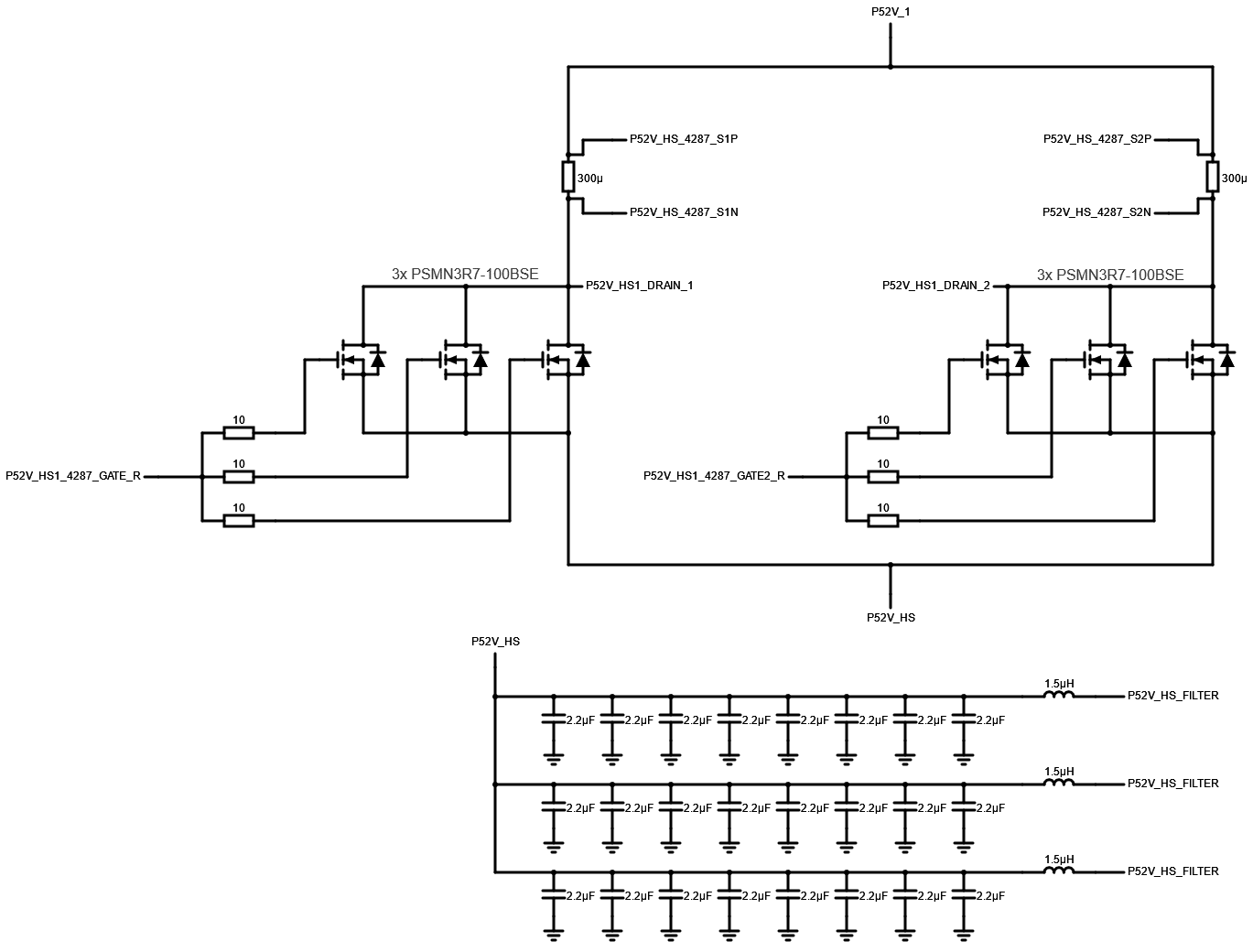
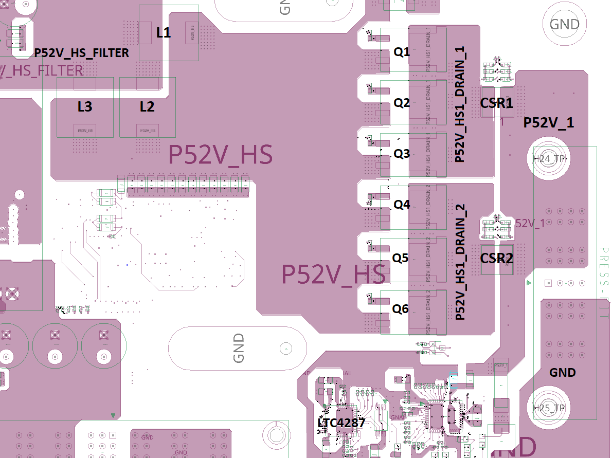
The P52V_1 net is where the 52V comes in on the right hand blade connector. It passes through a pair of 300μΩ current sense resistors, with kelvin connections to the LTC4287 for sensing the current on each leg. These form the P52V_HS1_DRAIN_1 and P523V_HS1_DRAIN_2 nets, each of which is switched by three Nexperia PSMN3R7-100BSE MOSFETs in parallel. The MOSFET gates are driven through 10Ω resistors, with each triplet driven by one of the LTC4287 gate drive channels. The six MOSFET sources all tie together to form the P52V_HS rail. This rail then feeds through three parallel 1.5μH power inductors to produce the P52V_HS_FILTER rail that is fed to the DC-DC bricks.
Here’s the PCB layout:
Naturally this seemed rather odd to me in the moment. Why would you use a dual-channel hotswap controller with just one rail? If it was just a case of switching the rail with some inrush control, a single channel with parallel MOSFETs would work just fine.
The answer turns out to be really clever! Since the LTC4287 has independent current sensing on each channel, it ends up balancing the current across each triplet of MOSFETs just like an ideal diode-OR. But, in this case, the goal isn’t just to ensure even power dissipation across the MOSFETs - it also ensures that the current density across the power planes is evenly spread.
Since current will generally flow through the most direct path, a single uninterrupted power plane would end up carrying very little current through the majority of its copper. By using a large number of parallel MOSFETs physically distributed across the plane, the current flow is more evenly distributed, resulting in lower power delivery network (PDN) impedance and fewer current density hotspots.
I decided to simulate this with Altium’s PDN Analyzer plugin. Here’s what the current density looks like when just a single plane is used, normalised to a scale of 0-100A/mm²:
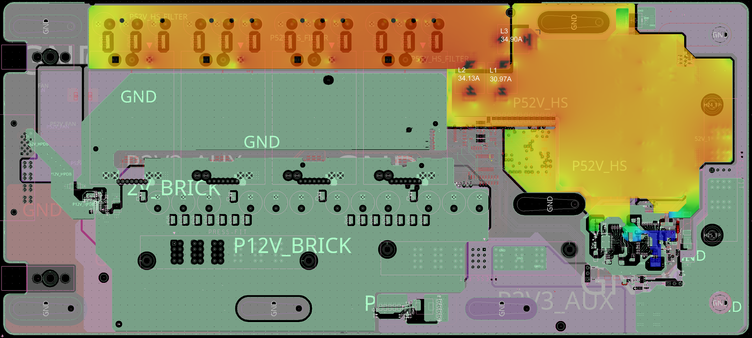
At 100A of load (25A per brick) the inductors carry 30.97A, 34.13A, and 34.9A respectively. Measured as a delta from the nominal 33.33A, that gives us -7.09%, +2.39%, and +4.7%. The magnitude of imbalance is 3.93A.
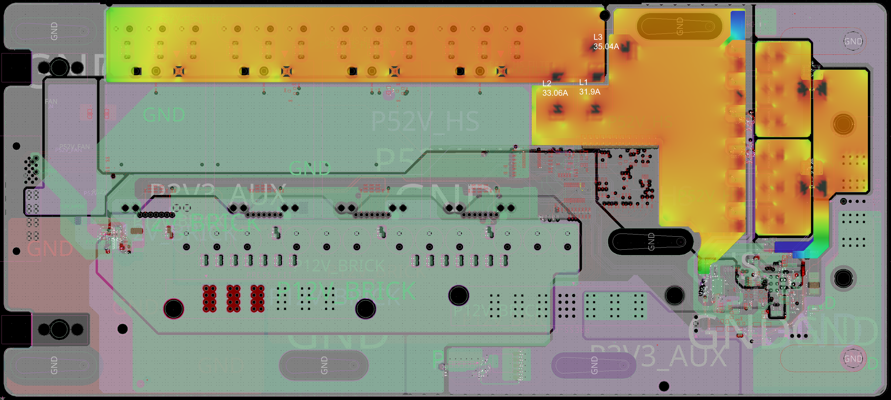
At the same 100A load, the inductors carry 31.9A, 33.06A, and 35.04A each. Measured as a delta from the nominal 33.33A, that gives us -4.3%, -0.82%, and +5.12%. The magnitude of imbalance is 3.14A.
The single-plane design ends up having about 50% more copper area than the design with the current balancing design. In hindsight I probably should’ve equalised the two areas, but it doesn’t matter a whole lot. Even with the extra copper, the balancer design produces less variation in the current density and reduces the imbalance across the inductors. Since they needed to include a hotswap controller anyway, this ends up being a really clever solution with negligible BOM cost.